Applied Radiology Focus: Digital diversity dilemma
Images
Recent advances in semiconductor manufacturing technology may be the "genie in the bottle" that every radiologist wishes for: Electronically readable X-ray detectors that can provide both excellent image quality and the capability of very rapid access to, enhancement of, and distribution of, the digital image output. Coupled with robust computer technology, digital radiography (DR) devices provide integrated direct readout of the image data and eliminate the time and equipment associated with film processing and development.
In many cases, the inherent efficiencies of digital technologies can lower the radiation dose. Patient throughput can be greatly increased; in fact, the time it takes to reposition the patient for a second image can actually exceed the cycle time of the device, which can be only a few seconds. There are many different methods used to capture and convert X-rays into electronic signals for immediate display, and the enviable digital dilemma facing radiologists now is to understand the many different detector and readout systems available through this emerging technology to enable an educated choice for their particular applications.
Flat-panel thin-film transistor arrays
To take full advantage of the development of large-area X-ray detectors, DR systems need integrated large-area readout mechanisms with sophisticated, but miniaturized, electronic circuitry to capture the electronic charge image data. The mechanism must be capable of low noise, wide dynamic range, and fast response. Thin-film transistor arrays make use of electronic microfabrication techniques to position electrodes for pixel charge collection and readout mechanisms in layers immediately adjacent to the site of the photon interactions, all within a protective enclosure, complete with cabling for computer connection. 1 Bias voltages channel the charges from the surface of the photodetector to the nearest collector electrode in the transistor array. Pixel separation is assured by electronic field shaping within the photodetector, which preserves spatial resolution and can produce a very high fill factor (approaching 100%). The electronic charge information is converted from analog to digital and processed by a computer for display on a monitor and storage in a DICOM-compliant form.
Components used in direct readout digital devices
Amorphous selenium
A photoconductor is a type of semiconductor that is an insulator under conditions of darkness but becomes a conductor when illuminated. The light-sensitive electrical properties of photoconductors make them useful in various devices, such as infrared detectors and video cameras. When X-rays strike a photoconductor, such as selenium, the energy of the incoming photons excites the low-energy selenium valance electrons, causing them to move into a higher energy state called the conduction band. The "holes" formed after the electrons are released can be thought of as positive charges that attract neighboring negatively charged electrons. 2 As electrons move into these holes, they leave new holes. These electron-hole pairs function as charge carriers. If an electric field is formed by positively charging one surface of the photoconductor, the released electrons and the holes will move along the applied field toward opposite surfaces of the photoconductor, where the electrons will cancel the positive surface charges (Figure 1). The resulting variations in the surface charge correspond to the incident pattern of the X-rays and faithfully reproduce the original X-ray image. This method of transforming X-ray energy directly into an electric charge is called direct conversion.
The photoconductive properties of selenium make it particularly well suited for use in digital radiography. It has a very low dark or leakage current, it forms approximately 1000 electron-hole pairs per 50 keV X-ray beam at an electric field of 10 volts per micron, and it has good attenuation of X-rays (~50% attenuation of a 50 keV beam with 365 microns of selenium; 50% attenuation of a 20 keV beam with 30 microns of selenium). 2 Advances in the manufacture of semiconductor materials has made it possible to make large surface area plates of selenium by evaporation of its amorphous form instead of earlier methods that relied on growing selenium crystals. This has made production of flat-panel sele-nium-based electronic X-ray detectors much more economical.
Amorphous silicon
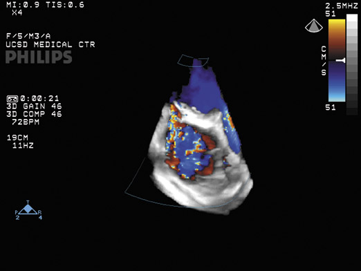
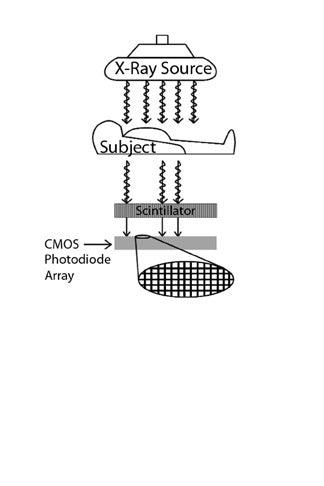
Amorphous silicon is also a photoconductor and can capture photons and generate electron-hole pairs. Unfortunately, silicon has a very low capability for absorption of high-energy photons, such as X-rays, and the detector would need to be 10- to 20-mm thick for most clinical radiography applications. 3 Fabricating amorphous silicon devices of this thickness is not practical, and so such arrays would need to be made of crystalline silicon, which is currently very expensive. However, silicon can capture and convert visible light photons very well. When used with scintillators, such as cesium iodide, that absorb X-rays efficiently and emit visible light near the peak of the spectral sensitivity of silicon, photodiodes made of amorphous silicon can function as charge storage devices. This digital capture method uses a 2-step process called indirect conversion to transform X-ray photons first to visible light and then to an electric charge (Figure 2). The thin-film transistor and an external voltage can be used as a switch to permit the charge to flow from the silicon photodiode when a readout is desired (other combinations of charge storage devices and switches can be used). An example of a clinical image made with this approach can be seen in Figure 3.
Scintillators
Scintillators convert detected X-ray photons into visible light. A good scintillator is an efficient producer of light photons: 20 to 50 visible photons out per 1 keV of incoming X-ray energy are typical. 3 Scintillators are usually made of a material with a high atomic number to achieve good X-ray absorption and an emitter substance that facilitates the conversion to visible photons. Some scintillators are crystalline, like cesium iodide. Scintillators such as gadolinium oxysulfide phosphors are granular, which can tend to scatter light and cause a loss of photons. Robin Windsor, CTO of Imaging Dynamics Company, explains "There are a lot of factors involved with designing a system so you do not get a 'quantum sink' effect, where you lose more light photons than the number of X-ray photons you started out with." One way to limit the loss of visible light through scattering is to restrict or channel the photons. Cesium iodide can be evaporated to form discrete, parallel needles <20 microns in diameter that act as crystalline conduits. 3 This structured design channels the photons and limits the spread of visible light, allowing a thicker scintillator layer to be used. The thicker the layer, the higher the X-ray absorption efficiency and the better the resolution. The visible light is next converted to an electric charge by various methods such as amorphous silicon photodiode circuitry, a charge-coupled device, or a complimentary metal- oxide semiconductor.
Charge-coupled devices
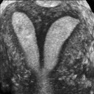
A charge-coupled device (CCD) is an integrated circuit composed of many light-sensitive cells (pixels) made of semiconductor material, typically silicon. The method by which the local charge is extracted from the original photon interaction site is reminiscent of the electron-hole pairs formed in the selenium photoconductor. Within the silicon crystal, electron storage sites or "potential wells" are formed by an electric field generated by voltages applied to electrodes on the surface of the CCD. By controlling the collapse and growth of adjacent wells, the charge can be "coupled" (output of one is input of the next) and moved from the original pixel to an integrated readout mechanism that assigns a digital value to the collected charge. 4 When CCDs are used via indirect conversion methods in digital radiography, X-ray photons are converted into visible light photons by a scintillator and directed to the CCD by means of a lens or fiberoptic taper. A mirror may be used to deflect the scintillator output and remove the sensitive electronics in the CCD from the path of the X-ray beam (Figure 4). An example of a clinical image made with this approach can be seen in Figure 5. Modern CCDs have overcome initial technological problems of thermal noise by using semiconductor Peltier coolers. Early Peltier coolers were based on the heat differential that develops between two dissimilar metals that have a current run across them, wherein one side gets hot and the other side gets cold. Today's solid state Peltier devices can cool CCD arrays, such as those in the Hubble space telescope, with no moving parts or coolant requirements (personal communication, Robin Windsor, March 2005).
Related Articles
Citation
Applied Radiology Focus: Digital diversity dilemma. Appl Radiol.
May 4, 2005